Semiconductor
APPLICATIONS

Semiconductor

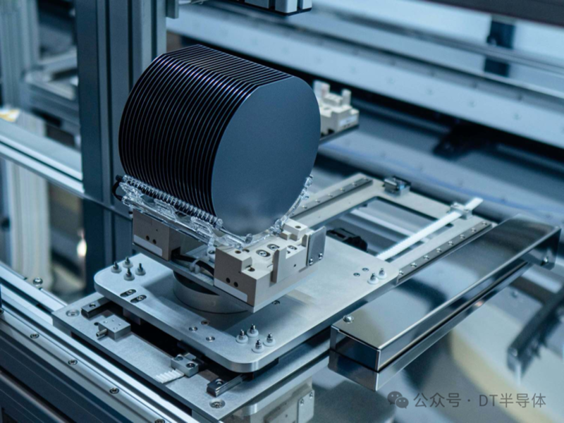
Diamond Abrasives for Semiconductor Wafer Processing

Diamond abrasives are widely used in semiconductor wafer grinding, lapping and polishing, where controlled material removal, dimensional accuracy and surface quality are critical.

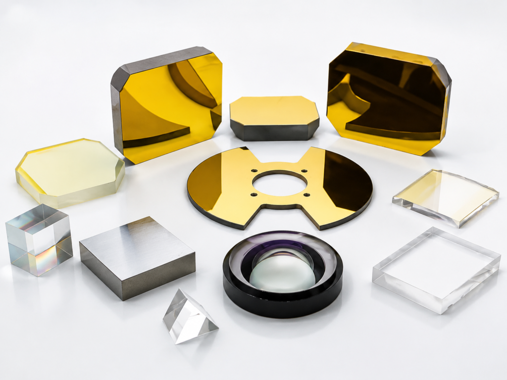
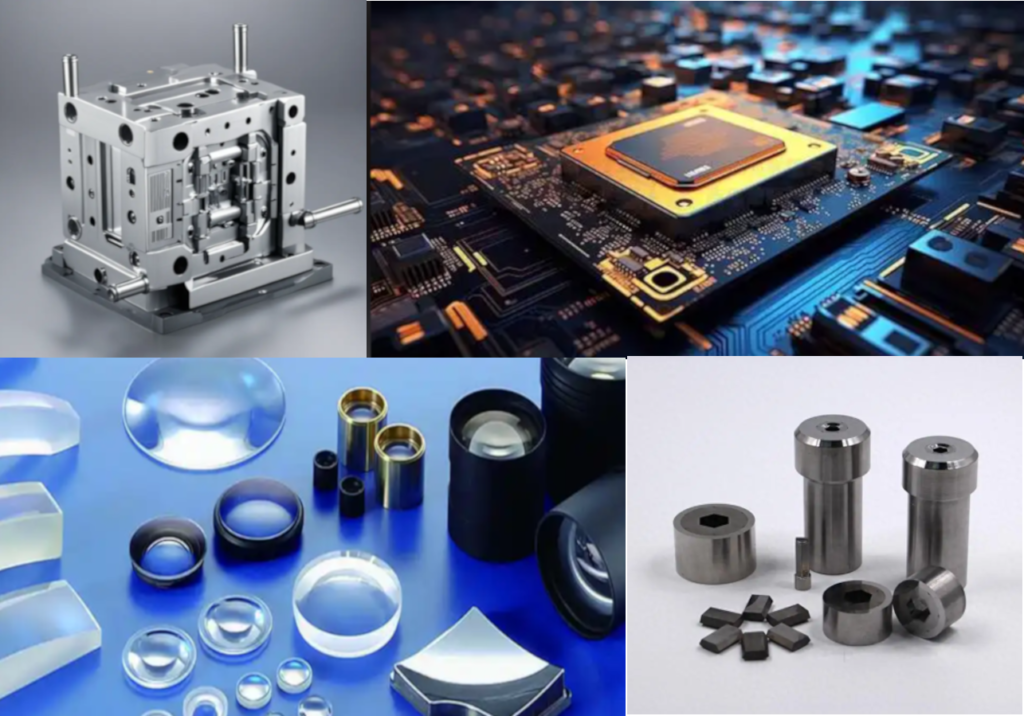
Crownkyn supplies diamond abrasive grades and formulated products for silicon, SiC, sapphire and other semiconductor substrates, with particle size, diamond type and product form matched to different processing stages and surface requirements.

Industry Challenges

Key processing challenges that influence abrasive selection and application performance.

Hard and Brittle Material Processing

SiC and sapphire are hard and brittle, requiring efficient material removal while limiting fracture and subsurface damage.

  • High hardness
  • Edge chipping
  • Subsurface damage

Surface Quality and Dimensional Control

Wafer processing requires tight control of flatness, thickness and surface quality as grinding progresses toward fine polishing.

  • Scratch control
  • Flatness consistency
  • Fine surface finish

Abrasive Consistency and Process Stability

Stable results depend on consistent particle size, shape and oversize control across abrasive batches.

  • Narrow PSD
  • Oversize control
  • Batch consistency

Recommended Processing Stages

Diamond abrasive type, particle size and product form can be matched to different processing stages to balance removal efficiency, dimensional control and final surface quality.

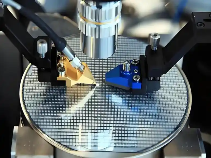
Wafer Slicing and Dicing

Wafer Slicing and Dicing

Diamond abrasives are used in slicing and dicing tools for hard and brittle semiconductor materials where cutting efficiency, edge quality and controlled material removal are required.

  • Wafer slicing and dicing: Select diamond grit according to substrate material, cutting method, wafer thickness and required edge quality.
  • Precision cutting: Finer, tightly controlled diamond particles help reduce chipping and subsurface damage.
  • Diamond selection: Particle size, PSD, morphology and strength should be matched to the specific tool and process.

Typical applications: Silicon, SiC, sapphire, GaAs and other hard substrate materials.
Wafer Grinding and Edge Processing

Wafer Grinding and Edge Processing

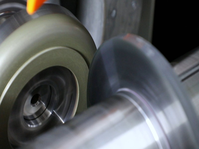
Diamond abrasives are used for wafer thinning, back grinding and edge processing, where controlled material removal must be balanced with dimensional accuracy and subsurface damage control.

  • Back grinding: Diamond abrasives for efficient wafer thinning and controlled material removal
  • Fine grinding: Finer, tightly controlled diamond grades for improved thickness consistency and reduced grinding damage
  • Edge processing: Selected diamond abrasives for edge shaping, beveling and controlled edge geometry

Typical applications: Wafer thinning, back grinding, edge grinding and substrate shaping.

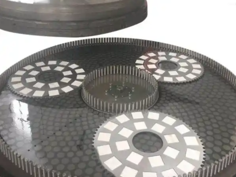
Lapping and Precision Polishing

Lapping and Precision Polishing

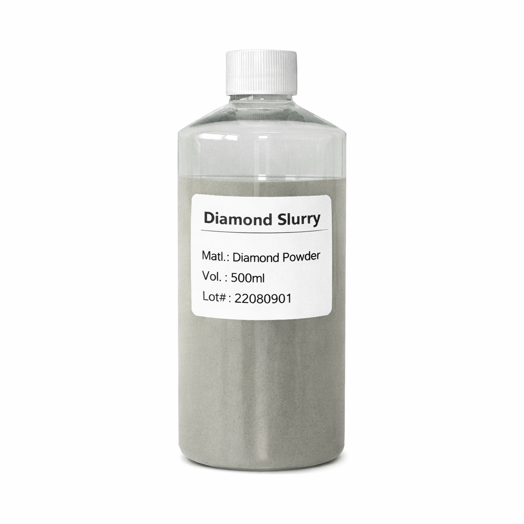
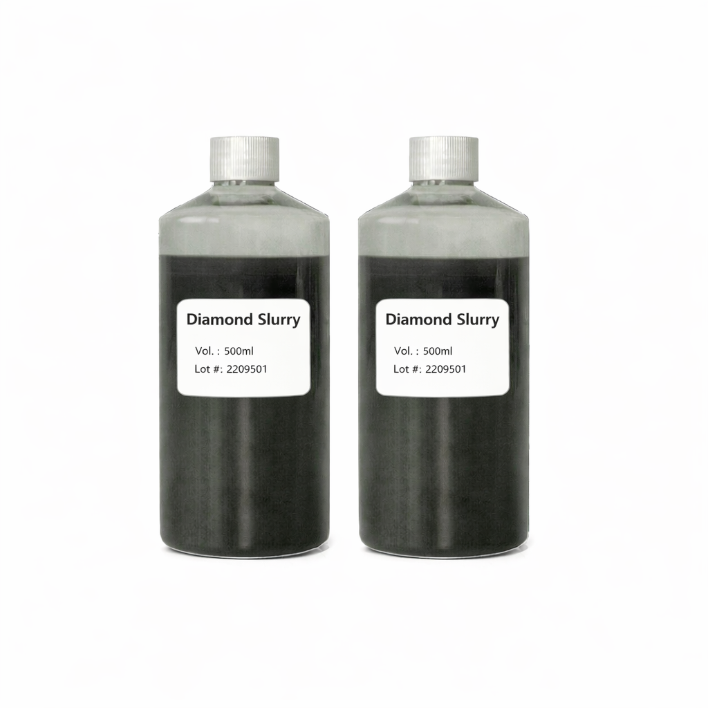
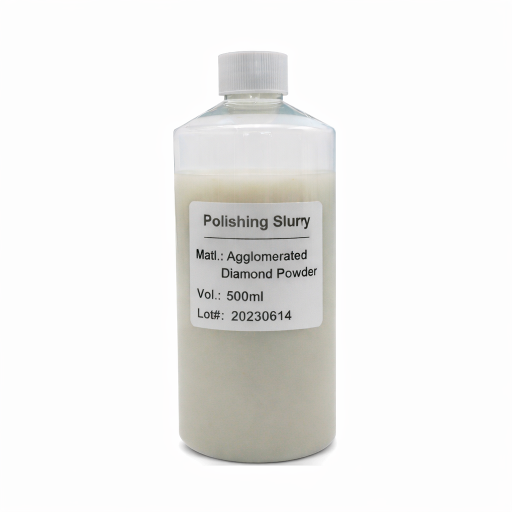
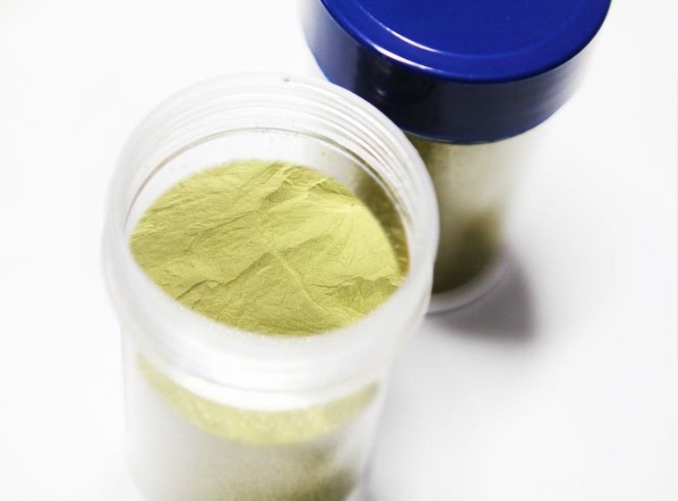
Micron diamond powder and diamond slurry can be used in lapping and precision polishing of hard semiconductor and substrate materials to progressively reduce grinding damage, improve flatness and achieve a controlled surface finish.

  • Pre-lapping: Coarser micron diamond for efficient removal of grinding marks and surface damage
  • Fine lapping: Controlled micron grades for improved flatness and progressively lower surface roughness
  • Precision polishing: Fine micron or submicron diamond where low defect levels and controlled surface finish are required

Typical applications: SiC, sapphire, ceramic and other hard substrate materials.
Ultra-Fine Surface Finishing

Ultra-Fine Surface Finishing

Submicron and nano diamond can support specialized ultra-fine finishing processes where very low surface roughness, tight particle-size control and minimal surface defects are required.

  • Submicron finishing: Fine diamond grades for reducing residual surface defects from preceding polishing stages
  • Nano-scale finishing: Nanodiamond for specialized processes requiring extremely fine abrasive action
  • Surface quality control: Tight PSD and oversize control help reduce scratching and improve finishing consistency

Typical applications: Advanced SiC, sapphire and specialty semiconductor substrate finishing.

Diamond Abrasive Selection for Semiconductor Processing

Select diamond abrasive type, particle size and product form according to the substrate material, processing stage and required surface quality.

Selection Factor
Selection Guidance
Selection Factor Substrate Material
Selection Guidance

Consider the hardness, brittleness and processing behavior of SiC, sapphire, silicon, GaAs and other semiconductor substrate materials.

Selection Factor Processing Stage
Selection Guidance

Match abrasive characteristics to slicing, back grinding, lapping, polishing or ultra-fine finishing requirements.

Selection Factor Diamond Type
Selection Guidance

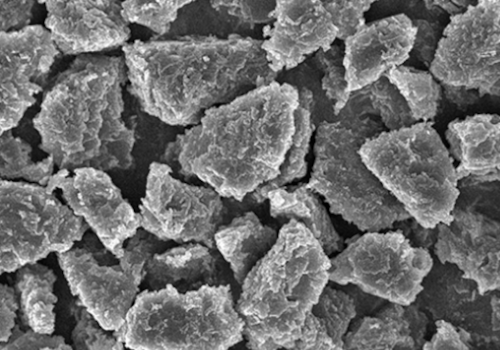
Select monocrystalline, crushed, coated or specialty diamond grades according to the tool system, removal requirement and finishing target.

Selection Factor Particle Size & PSD
Selection Guidance

Use coarser grades for efficient material removal and progressively finer micron, submicron or nano grades as surface-finish requirements increase. Tight PSD and oversize control help reduce scratching in fine finishing.

Selection Factor Product Form
Selection Guidance

Choose diamond powder for bonded tools or custom formulations, and slurry or paste for lapping and polishing processes requiring controlled abrasive dispersion.

Frequently Asked Questions

Common questions about selecting diamond abrasives for semiconductor wafer grinding, lapping and polishing.

Why is diamond abrasive used for SiC and other hard semiconductor wafers?

Diamond provides the hardness and cutting ability required to process hard, brittle substrates such as SiC, sapphire and GaN. It is widely used in grinding, lapping and polishing stages where efficient material removal must be balanced with surface quality and subsurface-damage control.

What diamond particle size is suitable for semiconductor wafer processing?

The suitable particle size depends on the wafer material and processing stage. Coarser abrasives support higher material removal during grinding or lapping, while finer micron and sub-micron grades are used as surface-finish and damage-control requirements increase.

What is the difference between monocrystalline and polycrystalline diamond for wafer polishing?

Monocrystalline diamond provides strong cutting edges and good wear resistance, while polycrystalline diamond contains multiple cutting points and can fracture progressively during polishing. The preferred type depends on the required removal rate, surface finish and sensitivity to scratching.

Should I use diamond powder or diamond slurry for wafer lapping and polishing?

Diamond powder is suitable when the user prepares or customizes the abrasive formulation internally. Ready-to-use diamond slurry provides controlled abrasive concentration, dispersion and carrier characteristics, making it more convenient for established lapping and polishing processes.

How can scratching and subsurface damage be reduced during wafer polishing?

Scratch and damage control depend on abrasive type, particle size distribution, oversize control, dispersion stability and polishing conditions. Clean processing equipment and preventing contamination between abrasive stages are also important for maintaining consistent wafer surfaces.

Is diamond slurry used for final CMP of semiconductor wafers?

Diamond slurry is commonly used for mechanical lapping, polishing and pre-CMP processing of hard substrates such as SiC and GaN. Final CMP typically relies on a material-specific chemical-mechanical slurry system, so diamond abrasive selection should be matched to the exact wafer material and process stage.

Need Help Selecting the Right Diamond Abrasive?

Share your application, processed material, current abrasive specification and target performance. Our team can recommend a suitable diamond product for evaluation.

Chat with us on WhatsApp