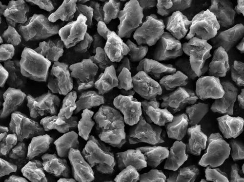
- Polycrystalline Diamond Structure: Multiple fine crystallites provide numerous cutting edges for controlled abrasive action.
- Fine Polishing of Hard Substrates: Suitable for precision surface finishing of SiC and selected other hard semiconductor materials.
- Controlled Surface Refinement: Multiple cutting edges support fine material removal and consistent surface finishing.
-
Self-Sharpening Characteristics:
Microfracture can expose fresh cutting edges
during polishing. - Selected Micron Grades: Fine particle sizes can be matched to different polishing stages and surface finish requirements.
- Customizable Formulation: Diamond concentration and water- or oil-based carrier options can be selected according to application requirements.
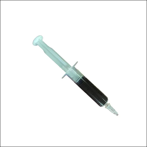
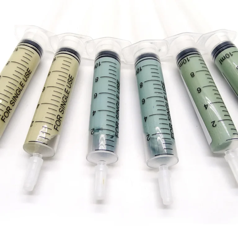
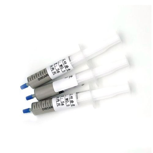
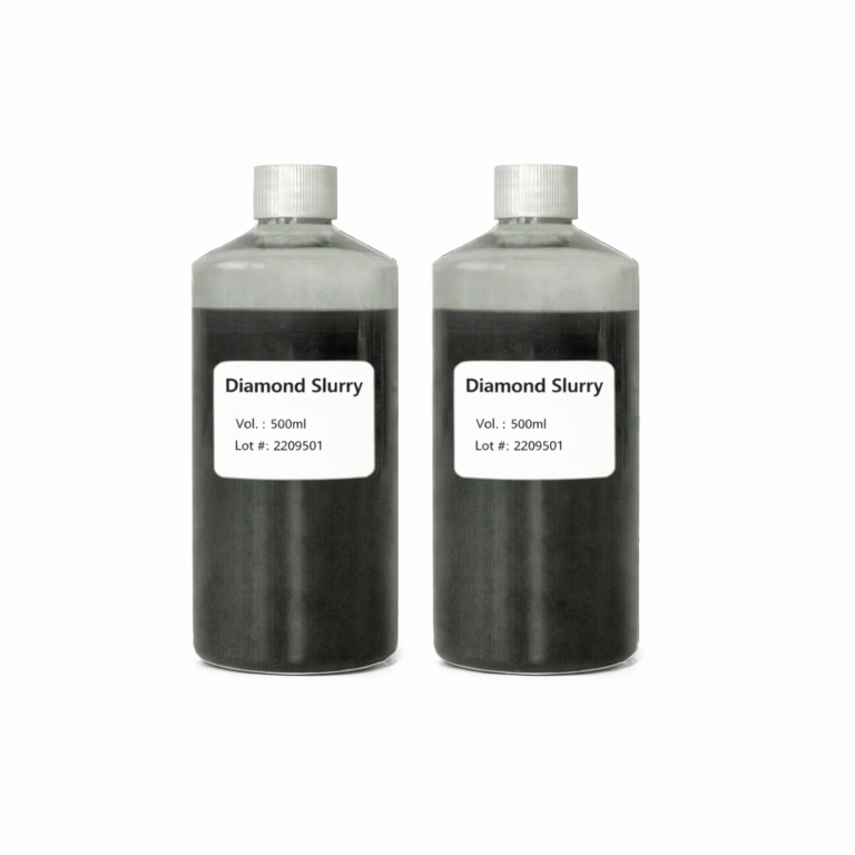
Polycrystalline Diamond Paste
20+ Years Experience
Consistent Batch Quality
Customized Solutions
Product Overview
Polycrystalline Diamond Paste is a precision polishing compound formulated with fine polycrystalline diamond abrasives for high-quality surface finishing of hard and difficult-to-polish materials. Its polycrystalline structure provides multiple fine cutting edges for controlled material removal and surface refinement. The paste is suitable for fine polishing of SiC and other selected semiconductor substrates, as well as sapphire, advanced ceramics and cemented carbides.
Features
Specifications
| Product Type | Polycrystalline Diamond Polishing Paste |
|---|---|
| Abrasive Type | Polycrystalline Synthetic Diamond |
| Particle Structure | Multiple Fine Diamond Crystallites |
| Available Particle Size | Selected Micron Grades, up to 12 μm |
| Particle Size Distribution | Controlled according to selected grade |
| Base Medium | Water-Based / Oil-Based |
| Concentration Options | Light / Medium / Heavy; customized diamond concentration available upon request |
| Primary Application | Fine and Precision Polishing of Hard Semiconductor Substrates and Other Hard Materials |
| Product Form | Ready-to-Use Polishing Paste |
| Selection Focus | Particle size, particle size distribution, diamond concentration, carrier type and target surface finish |
- Binder Type:
- Water-Based Polycrystalline Diamond Paste: Preferred for semiconductor, optical, and ceramic applications, offering fast cooling, easy cleaning, and no oily residue for clean processes.
- Oil-Based Polycrystalline Diamond Paste: Provides enhanced lubrication for soft or sticky metals, supports extended polishing time, and offers rust protection, with post-polishing cleaning recommended.
Polycrystalline Diamond Paste Particle Size Chart
|
Particle Size (μm) |
Reference Mesh / Grit No. (#) |
Reference W Grade |
Reference D50 (μm) |
Suggested Polishing Stage |
|---|---|---|---|---|
| 5–10 | 2000# | W10 | 6.5–7.3 | Precision Polishing |
| 4–8 | 3000# | W7 | 5.0–6.0 | |
| 3–6 | 4000# | W5 | 3.5–4.5 | Fine Polishing |
| 2–4 | 6000# | W3.5 | 2.2–2.6 | |
| 1–3 | 10000# | W2.5 | 1.6–1.8 | Ultra-Fine / Mirror Polishing |
| 1–2 | 12000# | W1.5 | 1.1–1.3 | |
| 0–1 | 15000# | W1.0 | 0.6–0.8 | |
| 0–0.5 | 30000# | W0.5 | 0.2–0.3 |
Note: Grit numbers, W grades and D50 values are for reference. Custom particle sizes and formulations are available upon request.

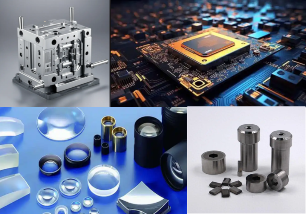
Applications
Semiconductor
Used for fine mechanical polishing of SiC and other selected hard semiconductor substrates where controlled material removal and surface quality are important.
- SiC wafer and substrate fine polishing
- Precision finishing of semiconductor substrate samples
- Fine surface refinement of hard crystalline materials
Optical & Optoelectronic
Used for precision polishing of sapphire and selected optical crystals requiring controlled material removal and fine surface finishing.
- Sapphire substrate fine polishing
- Precision finishing of hard optical crystals
- Surface refinement of optoelectronic components
Cemented Carbides
Used for fine polishing of cemented carbide specimens during metallographic preparation and microstructural examination.
- Tungsten carbide metallographic specimen polishing
- Polishing of prepared carbide cross-sections
- Surface preparation for microstructural examination