Comprehensive Overview of Synthetic Diamonds in 2026
For centuries, people have seen diamonds as nature’s ultimate wonder, born from time, pressure, and pure chance. These stones formed billions of years ago, about 150 kilometers below the Earth’s surface, and were carried up by ancient volcanic eruptions. That origin gave them an air of romance, rarity, and strength. Owning a diamond felt like holding a piece of the planet’s deep history.
Yet, in a quiet revolution spanning the last three decades, laboratories have learned to do in decades what nature takes eons to complete. Today, synthetic diamonds are chemically, physically, and visually identical to mined ones and they’re starting to change everything, from the sparkle on an engagement ring to the core of a quantum computer that needs to dissipate heat. This is not a story of cheap imitation. This is a story about engineering at its most impressive.
Chapter 1: Defining the Real Thing - What Synthetic Diamonds Are
Before exploring how these diamonds are made, let's clear up a common misunderstanding: a synthetic diamond is not a fake diamond.
Common simulants like cubic zirconia (CZ) or moissanite are diamond imitations. They look similar to the untrained eye, but their chemical composition (zirconium dioxide or silicon carbide) is entirely different from a diamond’s pure carbon lattice. A synthetic diamonds, on the other hand, is a real diamond. It has carbon atoms arranged in the same crystal structure as a natural diamond. It's just as hard, scoring a perfect 10 on the mohs scale, exhibits the same high thermal conductivity (900–2,320 W·m⁻¹·K⁻¹), and bends light with the same high refractive index (2.42) and dispersion (0.044).
The only real difference is where it came from: one was shaped by heat and pressure deep in the Earth, the other by human skill inside a manufacturing plant.
What we mean by 'synthetic'
The industry uses several terms interchangeably:
- Synthetic diamond (the scientific and FTC-preferred term)
- Lab-grown diamond (the consumer-friendly marketing term)
- Man-made diamond (industrial descriptor)
- Cultured diamond (evoking parallels with cultured pearls)
All are acceptable. What matters is the underlying reality: synthetic diamonds are diamonds, atom for atom.
Chapter 2: The Three Ways: Pressure, Gas, or Explosion
Nature has one way to make diamonds: extreme pressure and heat. Humanity has developed two primary routes, plus a specialized third method for unique applications.
2.1 High Pressure-High Temperature (HPHT): Mimicking the Mantle
The HPHT method was the first way synthetic diamonds were successfully created by man and was commercialized by General Electric in 1954. It directly simulates the Earth's deep mantle conditions.
How It Works
A small diamond "seed" crystal is placed inside a reaction cell, surrounded by a carbon source (typically high-purity graphite). This cell is loaded into a massive hydraulic press (this can be a belt press, cubic press, or toroid-type press). The press then applies two simultaneous forces:
- Pressure exceeding 5.5 GPa (gigapascal). For reference, 1 GPa is roughly 10,000 times atmospheric pressure. At 5.5 GPa, we are approaching the pressure found 150–200 km deep inside the earth.
- Temperatures above 1,400°C – hot enough to melt iron, nickel, or cobalt catalysts.
Under these conditions, the graphite dissolves into a molten metal flux (typically iron-nickel-cobalt). Carbon atoms migrate through this molten metal and precipitate onto the cooler diamond seed, growing the crystal layer by layer. This process runs for days or even weeks, depending on the desired size of the finished synthetic diamond.

Key Characteristics
Growth Rate: HPHT can grow diamonds relatively quickly, up to 0.5 carats per day for small stones.
Typical Colors: Due to nitrogen impurities absorbed from the atmosphere or the metal flux, HPHT diamonds often appear yellow, brown, or greenish. Adding boron during growth yields blue diamonds (the same mechanism that colors natural Type IIb blue diamond).
Inclusions: The most diagnostic feature is metallic flux inclusions. Under magnification, one can see tiny, dark, rod-like or spherical particles of metal catalyst that failed to escape the crystal. These are never found in natural diamonds (which contain mineral inclusions like garnet or peridotite).
Magnetism: Because of these metallic inclusions, many HPHT diamonds are slightly magnetic, a property natural diamonds lack.
Applications
HPHT diamond is the workhorse of industrial diamond production. The majority of diamond grit used in saw blades, drill bits, and grinding wheels is HPHT diamond based. This dominance comes down to three factors: low cost, robust process, and well-established quality control. HPHT presses can run continuously for days or weeks with minimal intervention, manufacturers can produce tons of diamond grit each year at a fraction of the cost of natural diamond mining. The resulting crystals may be small and imperfect by gemstone standards, but for cutting granite, drilling through rock, or grinding hardened steel, they are perfectly suited. Beyond industrial diamond grit applications, HPHT is also used to produce gem-quality diamonds. However, the as grown crystals can appear yellow, brown, or greenish in colour due to nitrogen impurities absorbed from the metal flux or surrounding atmosphere. To turn these into the colorless or near-colorless stones that consumers prefer, manufacturers typically send the rough diamonds through an additional post-growth treatment often a second HPHT run under different conditions. This annealing process rearranges the nitrogen impurities or heals lattice defects, resulting in a much clearer, more marketable stone. Some manufacturers also use HPHT to intentionally create different colors in the gemstone: adding boron during growth produces striking blue diamonds, while specific pressure-temperature paths can yield pink or red hues.
2.2 Chemical Vapor Deposition (CVD): Building from Gas
If HPHT is considered a high-pressure forge, CVD is a more gentle assembler. Developed in the 1980s and refined over the past two decades, C has become the preferred method for high-purity, large, flawless gemstones and electronic-grade synthetic diamonds.
How It Works
A diamond seed is placed in a vacuum chamber. The chamber is then filled with a carbon-rich gas mixture typically consisting of:
- Methane (CH₄) – as the carbon source
- Hydrogen (H₂) – in great excess (often 99% hydrogen to 1% methane)
Energy - either from microwaves, a hot filament, or a plasma torch is then introduced. This energy dissociates the hydrogen molecules into atomic hydrogen. Atomic hydrogen is highly reactive; it strips away any non-diamond carbon (graphite) from the seed's surface while allowing carbon atoms from the methane to settle and bond in the diamond lattice.
Crucially, the process occurs at low pressure (typically 0.1 to 10 torr, far below atmospheric pressure) and moderate temperatures (700–1,000°C). Carbon atoms deposit one atomic layer at a time, The diamond grows in a way that perfectly matches the atomic structure of the seed, so the new crystal continues the same pattern atom by atom.

Key Characteristics
Purity: CVD produces Type IIa diamond, the purest form, containing virtually no nitrogen or boron impurities. Type IIa is optically colorless, UV-transparent, and has the highest thermal conductivity.
Inclusions: High-quality CVD diamonds are inclusion-free. However, lower-quality runs may show pinholes or graphitic inclusions from incomplete etching. A unique feature is stria—growth lines visible under certain lighting that indicate the layered deposition process.
Color: As-grown, CVD diamonds are typically brownish due to defects in the lattice (vacancy clusters). These brown hues are almost entirely removed by a subsequent HPHT annealing process, which heals lattice defects and yields colorless or near-colorless stones.
Size: CVD excels at producing large, single-crystal plates. Wafers up to 10 inches (250 mm) in diameter have been demonstrated, though commercial products are typically 1–2 inches for electronics and 3–4 carats for gemstones.
Spectroscopic Fingerprint: For gemologists, CVD diamonds have a definitive test: a sharp absorption line at 737 nm (nanometers) corresponding to a silicon-vacancy (SiV) center. Silicon is not naturally found in the diamond lattice; it comes from trace contamination (silicon from quartz windows or chamber walls) during the CVD process.
Applications
CVD is the leading method for gem-quality synthetic diamonds intended for jewelry. The controlled, low-pressure gas environment allows for minimal contamination, resulting in Type IIa diamonds—the purest classification, which is exceptionally rare in nature. For jewelers and consumers alike, CVD offers a diamond that is indistinguishable from the finest natural stones, at a fraction of the cost and with complete certainty that no mining was involved.
Beyond jewelry, CVD diamonds have become critical components in advanced electronics. Their extreme thermal conductivity allows them to act as heat spreaders in high power lasers, radio frequency devices, and quantum computing components. In these applications, heat is the enemy; even small temperature rises can shift laser wavelengths or cause qubits to lose coherence. A CVD diamond placed next to a hot transistor or laser diode draws heat away efficiently, keeping the device stable and reliable. No other material performs this role as effectively.
Finally, the ability to grow diamond wafers—single-crystal plates up to 10 inches in diameter—makes CVD the preferred choice for research and advanced industrial applications requiring high purity. Scientists use CVD diamond as windows for high-power infrared lasers, as electrodes in harsh electrochemical environments, and as substrates for next-generation semiconductor devices. The process can be tuned to introduce specific impurities such as nitrogen for quantum sensing or boron for electrical conductivity—opening doors to technologies that were purely theoretical a decade ago. For these reasons, CVD has moved beyond the jewelry store and into the heart of the high-tech laboratory.
2.3 Detonation Synthesis: Diamond from Explosives
Not every application requires a beautiful, flawless single crystal. For grinding, lapping, and polishing, engineers need toughness and self-sharpening behavior. One of the most extraordinary ways to achieve this comes not from a press, but from an explosion.
How It Works
Detonation synthesis uses high explosives to convert carbon directly into diamond. The process begins with a carefully prepared explosive charge that contains a source of carbon, typically graphite or a carbon-rich organic compound. This charge is placed inside a sealed steel chamber, often filled with a protective or cooling atmosphere such as carbon dioxide, water, or nitrogen.
When the charge is detonated, two things happen almost instantly. First, a supersonic detonation wave travels through the explosive, generating enormous pressure (usually in the 20 to 30 gigapascals range), and in some setups reaching up to 50 gigapascals. Secondly, the chemical reaction of the explosive itself produces temperatures between 3,000 and 4,000°C. These extreme conditions last for only microseconds, but that is enough.
The key to the process is that the detonation wave compresses the carbon source faster than it can escape. Under these transient high-pressure, high-temperature conditions, the atomic structure of some of the carbon collapses from the hexagonal lattice of graphite (or amorphous arrangement of organics) into the cubic lattice of diamond. This transformation is not equilibrium growth—it is a shock-induced, kinetic process.
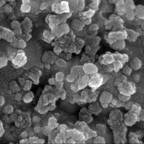
Critically, the resulting diamond does not form as large crystals. Instead, because the reaction happens so rapidly and then stops just as fast, the diamond emerges as millions of tiny diamond crystals, each typically between 5 and 100 nanometers in size, fused together into irregular, porous particles. The explosive conditions the detonation velocity, chamber atmosphere, carbon source purity, and coolant flow, can be tuned to control the average crystal size and the ratio of diamond to non-diamond carbon (such as graphite or amorphous carbon).
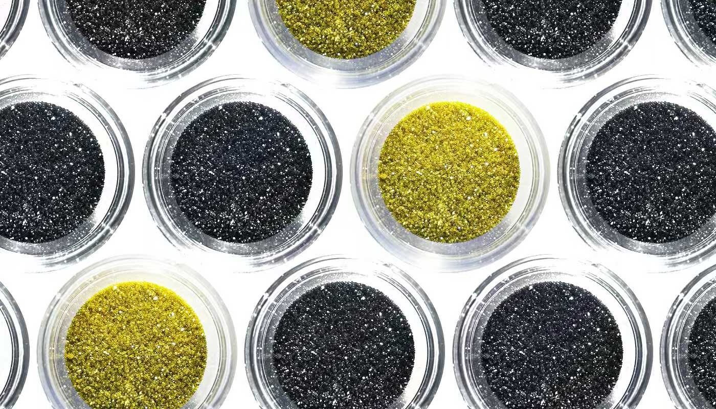
After the explosion, the soot-like product—known as detonation nanodiamond (DND)—is collected from the chamber walls and subjected to a series of purification steps: acid washing to remove non-diamond carbon and metal impurities from the explosive residue, followed by centrifugation and drying.
Key Characteristics
Nanocrystalline Size: The individual crystallites are 5–100 nanometers, making Detonation nano diamond (DND) ideal for ultra-precision polishing where micron-scale scratches are unacceptable.
Efficiency: A single detonation lasts only microseconds yet converts a significant fraction of the starting carbon into diamonds, making the process surprisingly efficient for such violent conditions.
Uniform Surface Finish: When used to polish hard materials like ceramics, tungsten carbide, or aerospace alloys, the Nanocrystalline nature of detonation nano diamond produces a finer, more uniform surface finish with far fewer deep scratches compared to monocrystalline grit.
Self-Sharpening: As a grain is used in a grinding or polishing application, the tiny nanocrystals at its surface fracture and exfoliate individually, constantly exposing fresh, sharp edges. This stands in contrast to monocrystalline diamond, which tends to cleave along flat crystal planes and develop dull, polished facets.
No Cleavage Planes: Since the material is a random polycrystalline aggregate with no long-range crystal orientation, it lacks the directional cleavage planes of single-crystal diamond. This makes it significantly tougher under impact and shear stress—the grains crush rather than split.
Applications
Detonation nano diamond (DND) is the material of choice for several high-precision industrial applications. In optics and electronics, it is used for precision lapping of optical fibers, where its self-sharpening nano diamond create exceptionally smooth ends for efficient light transmission. It is also the preferred abrasive for polishing aluminum nitride and silicon carbide substrates two materials critical to high-power electronics and LED manufacturing. Unlike conventional abrasives that leave deep scratches or chipped edges, detonation nano diamond produces a uniform, defect-free surface finish.
In heavy industry, this same material plays a vital role in drilling and machining. It is used for grinding polycrystalline diamond compact (PDC) cutters, which are the business end of oil and gas drilling bits. Detonation nano diamond is tough and lacks cleavage planes, it can shape and sharpen PDC cutters without introducing micro-fractures that would fail under extreme downhole conditions.
Finally, detonation nano diamond has found its way into advanced chemical-mechanical polishing (CMP) of semiconductor wafers, where even a single microscopic scratch can ruin a chip. Beyond polishing, it is also incorporated into high-performance lubricants where detonation nano diamond rolls between moving surfaces, reducing friction and into composite additives, where it reinforces polymers, metals, and coatings with diamond like hardness. In all these roles, what looks like a simple black powder turns out to be one of the most versatile engineering materials ever made.
Chapter 3: The Syntheic Diamond Comparisons – HPHT vs. CVD vs. PCD
To choose the synthetic diamonds for a given job, one must understand the trade-offs. The following table provides a technical summary:
| Feature | HPHT Diamonds | CVD Diamonds | PCD (Detonation) |
|---|---|---|---|
| Growth Method | High pressure (5.5+ GPa), high temperature (>1,400°C) | Low pressure, moderate temperature (700–1,000°C) | Explosive shockwave conversion |
| Crystal Structure | Single crystal | Single crystal (epitaxial layer) | Polycrystalline (nanocrystalline aggregate) |
| Typical Purity | Type Ib (nitrogen-rich) or IIb (boron-doped) | Type IIa (ultra-pure, no nitrogen) | Mixed, but dominated by nanocrystalline defects |
| Typical Color | Yellow, brown, blue, green | Brown (as-grown), colorless (after anneal) | Dark gray to black (opaque) |
| Key Inclusions | Metallic flux particles (magnetic) | SiV center (737 nm line), pinholes, stria | None at visible scale; nanoscale grain boundaries |
| Hardness (GPa) | 70–120 | 70–120 | 80–110 (lower than single crystal, but tougher) |
| Thermal Conductivity | Very high (1000–2000 W/m·K) | Highest (2000+ W/m·K for Type IIa) | Moderate (due to grain boundary scattering) |
| Primary Use | Industrial grit, cheap gemstones, cutting tools | Large flawless gems, electronics, heat sinks, quantum sensors | Precision grinding, lapping, polishing of hard materials |
| Relative Cost | Low (industrial) to medium (gem) | Medium to high (larger stones) | Low to medium (per kilogram) |
Chapter 4: Uses That Go Far Beyond Jewelry
While consumers are now seeing synthetic diamonds as a more affordable, ethical jewellery and ring option, the true revolution is happening in factories, laboratories, and semiconductor fabrications.
4.1 Industrial & Manufacturing (The Largest Market by Volume)
Over 90% of synthetic diamonds produced are not destined for jewelry they are aimed at the industrial abrasives markets.
- Cutting, Drilling, and Grinding: Diamond-tipped saw blades for cutting granite and asphalt; impregnated diamond drill bits for mining and construction; diamond grinding wheels for machining hardened steel, ceramics, and cemented carbides. HPHT diamond grit dominates here.
- Polishing and Lapping: The semiconductor industry consumes enormous quantities of diamond slurries to polish silicon wafers, sapphire substrates (for LEDs), and hard disk drive platters. Micron-sized PCD powders are preferred for final polishing because they produce fewer microscratches.
- Wire Drawing: Diamond dies—small single-crystal diamonds with a precisely drilled hole—are used to draw copper, tungsten, and gold wire down to hair-thin diameters. CVD diamond’s lack of inclusions makes it ideal for ultra-fine wire dies.
4.2 Thermal Management (The Electronics Revolution)
Modern electronics are always fighting one large issue: heat. As transistors shrink and power densities rise, conventional heat sinks (copper, aluminum) cannot remove heat fast enough. Diamond conducts heat five times better than copper and is electrically insulating (unless intentionally doped).
- Heat Spreaders: Thin CVD films (50–500 microns thick) are brazed ontoigh-power laser diodes, RF GaN transistors in 5G base stations, and LED arrays. By spreading heat laterally, diamond lowers junction temperatures, increasing device lifetime and output power.
- Substrates for GaN-on-Diamond: Researchers now grow gallium nitride (GaN) transistor layers directly on CVD substrates. The result: transistors that can handle 3–5 times higher power density before failing compared to those on silicon or silicon carbide.
4.3 Optics and Windows
Diamond is transparent from deep ultraviolet (225 nm) to far infrared (over 25 microns), with only one narrow absorption band near 5 microns. It is also the hardest optical material known.
- Infrared (IR) Windows: High-power CO₂ lasers (10.6 microns) used in cutting and welding require protective windows that transmit IR light while surviving laser scatter and debris. Synthetic diamond windows are standard in industrial CO₂ lasers. Similarly, military thermal imaging systems use diamond windows for missiles and drones operating in sandstorm or particulate-heavy environments.
- X-ray Windows: In synchrotrons and X-ray fluorescence analyzers, thin diamond windows (50–100 microns) allow X-rays to pass while maintaining a vacuum seal. Diamond’s low atomic number means minimal X-ray absorption and scattering, unlike beryllium (the traditional material, which is toxic and brittle).
4.4 Quantum Technologies (The Cutting Edge)
Here, synthetic diamonds do something nature never intended: they host quantum bits (qubits). The Nitrogen-Vacancy (NV) center is a defect in the diamond lattice where a nitrogen atom sits next to an empty lattice site (a vacancy). This defect has an electron spin that can be initialized, manipulated with microwaves, and read out using red laser light—all at room temperature. Natural diamonds rarely contain usable NV centers in controlled locations. synthetic diamonds, especially CVD, can be engineered with precise NV center density and depth.
- Quantum Sensors: A diamond tip with a single NV center can measure magnetic fields with nanoscale spatial resolution and sub-microtesla sensitivity. Applications include mapping current flow in integrated circuits, imaging magnetic domains in spintronic materials, and even detecting the magnetic field from a single neuron firing.
- Nanoscale Thermometry: The NV center’s spin resonance frequency shifts with temperature. A diamond nanocrystal containing NV centers can act as a fluorescent thermometer with sub-degree Kelvin precision, inserted into living cells.
- Diamond Anvil Cells (DACs): While not quantum per se, DACs use two brilliant-cut HPHT diamonds to squeeze a tiny sample between their tips, generating pressures exceeding 300 GPa—higher than the Earth’s inner core. Researchers use DACs to study the phase behavior of hydrogen (metallic hydrogen), superconductivity in hydrides, and the mineralogy of exoplanets.
4.5 Biomedical Applications (Emerging)
Diamonds is biocompatible, non-toxic, and resists protein adsorption and bacterial adhesion.
- Nanodiamond Drug Delivery: Detonation nano diamond (4–5 nm diameter) have high surface areas and can be functionalized with drug molecules. They are being tested for sustained release of chemotherapeutics (e.g., doxorubicin) with fewer side effects.
- Coatings for Implants: Thin CVD coatings are deposited onto titanium hip and knee implants, reducing wear debris (a major cause of long-term implant failure) and lowering infection rates.
- Neural Interfaces: Diamond electrodes are far more stable than metal or silicon electrodes for recording neural signals over months or years. They do not corrode, and they form a low-impedance interface with neural tissue.
Chapter 5: How Gemologists Tell Them Apart
To the naked eye, a flawless CVD diamond is indistinguishable from a flawless natural diamonds. Even a jeweler with a loupe cannot be certain. However, sophisticated gemological labs (GIA, IGI, HRD) use several methods:
| Test | Natural Diamond | HPHT Synthetic | CVD Synthetic |
|---|---|---|---|
| UV Fluorescence (longwave) | Typically blue, sometimes inert or yellow | Often green, yellow, or strong blue with a cross-shaped pattern (due to sectorial growth) | Typically orange, pink, or inert; often shows layered fluorescence stripes |
| Phosphorescence | Rare (seconds) | Common (minutes) after UV exposure | Rare or weak |
| Magnetism | Non-magnetic | Weakly to moderately magnetic (metallic inclusions) | Non-magnetic (no metal) |
| Microscopic Inclusions | Mineral crystals (garnet, peridotite, diamond) | Metallic flux particles (dark, rod-like) | Graphitic pinholes, stria lines, no metals |
| Spectroscopy (FTIR) | Type Ia (nitrogen aggregates) common | Type Ib (single substitutional nitrogen) or IIb (boron) | Type IIa (no detectable nitrogen) |
| UV-Vis-NIR Spectrum | Natural-specific absorptions (e.g., N3 center at 415 nm) | None typical; may show Ni or Co-related lines | Sharp SiV peak at 737 nm |
Chapter 6: The Future - Where Are Synthetic Diamonds Headed?
While the technology is still relativly young. Costs continue to fall by for CVD machinery, equipment and process consumables. Maximum sizes increase steadily: where 1-carat CVD gems were remarkable in 2010, 10-carat flawless stones are commercially available today. Wafers of 4 inches are routine for electronics; 6 and 8 inches are in development.
6.1 Diamond Batteries (Beta-Voltaics)
Researchers are combining radioactive isotopes (typically nickel-63 or carbon-14) with diamond's radiation hardness to create beta-voltaic batteries. When a beta particle (high-energy electron) strikes diamond, it creates electron-hole pairs, generating an electrical current. Because diamond is the most radiation-hard material known, these batteries can operate for decades without significant degradation. The first commercial diamond batteries are expected in the mid-2030s for pacemakers, remote sensors, and spacecraft.
6.2 Large-Area Diamond Electronics
Silicon works well, but it has limits. When temperatures rise above 200°C or voltages exceed 1,000 volts, silicon starts to break down. Diamond, on the other hand, can handle far more. Thanks to its ultra-wide bandgap a property that basically measures how much energy it takes to kick an electron loose, diamond can theoretically manage voltages up to 100,000 volts and temperatures over 800°C. That's a massive jump. Engineers have already built working prototype devices like diamond Schottky diodes and transistors. The problem is that diamond can be difficult to dope, that is, to add specific impurities that create the positive and negative regions needed for electronic devices. And large, high-quality diamond wafers are still very expensive. If researchers can solve those two challenges, diamond could eventually replace silicon in electric vehicle inverters, electrical substations, and power electronics for aircraft and spacecraft.
6.3 Advanced Polishing Slurries
The future of PCD and nanodiamond powders lies in surface functionalization. By attaching specific chemical groups (carboxyl, hydroxyl, amine) to nanodiamond surfaces, manufacturers can tailor dispersion stability in water, oil, or polymer matrices. For example, hydrophilic nanodiamonds remain suspended in aqueous slurries for months without settling, enabling consistent polishing in semiconductor chemical-mechanical polishing (CMP) processes.
6.4 Carbon Neutral Diamond
One persistent criticism of lab-grown diamonds is their energy intensity. A CVD reactor running for weeks at 1,000°C consumes tens of kilowatts of power. However, because the process is electrical, it can be powered by renewable energy (solar, wind, hydro). Several producers now market "carbon-neutral" or "carbon-negative" diamonds, using solar power and direct air capture of CO₂ for their methane feedstock. This is something mined diamonds can never claim.
Final Note for Buyers and Engineers
If you are looking to source synthetic diamonds for industrial use, do not simply ask for “diamond powder.” The right product depends entirely on your application. Please provide these specifications:
- Particle Size: Specify in microns (e.g., 0–0.5 µm for polishing, 40–50 µm for lapping, 100–200 µm for cutting) or mesh number. For nanodiamond, specify exact mean diameter (e.g., 5 nm, 10 nm).
- Purity Grade:
- Standard (98–99% diamond) – For general grinding, drilling, and sawing.
- High purity (99.9%+) – For electronics, optics, and precision lapping where metallic contamination is unacceptable.
- Crystal Morphology: Blocky (for maximum strength), sharp/irregular (for aggressive cutting), or polycrystalline (for self-sharpening, fine finishing).
- Surface Treatment:
- Nickel or copper plating – Improves retention in metal-bonded grinding wheels.
- Hydrophilic coating – For water-based polishing slurries.
- Untreated – For resin-bonded tools or oil-based slurries.
- Application Usage: Tell us whether you are grinding tungsten carbide, sawing granite, polishing silicon wafers, or machining carbon fiber composites. We can then recommend the optimal type of diamond (HPHT grit, CVD flake, or PCD powder).
Conclusion: The Diamond Age Has Arrived
For millennia, we were at the mercy of geology. If we wanted a diamond, we had to find a kimberlite pipe, blast open the rock, and sift through tons of ore for a few gem-quality stones. Today, we grow diamonds in clean rooms. We engineer their impurities, control their shape to the micron, and deploy them not as ornaments but as enablers of lasers, quantum sensors, and next-generation power electronics.
Synthetic diamonds are no longer a curiosity. They are a mature, growing, and technologically critical industry. Whether you need the self-sharpening toughness of polycrystalline diamond powder for a grinding operation, the ultra-pure thermal conductivity of a CVD wafer for a 5G base station, or the ethically sourced sparkle of a lab-grown engagement ring, the Synthetic diamonds.
Nature takes millions and millions of years to forge diamonds. Humanity has learned to do it in weeks. And in many ways, we have already we are now surpassing nature’s original design.