# What Makes Boron-Doped Diamond Unique?
You want the hardest material on earth, but you also need electricity to flow through it. Standard diamond fails at this task completely. It creates a frustrating limitation for advanced engineering projects that need durability and power.
**Boron-doped diamond (BDD) solves this by introducing boron atoms into the carbon lattice. This turns an insulator into a semiconductor or conductor. It combines diamond’s extreme hardness and chemical stability with excellent electrochemical properties, making it ideal for wastewater treatment and advanced electrodes.**
I have seen many people struggle to understand this material because it sounds like science fiction. I will explain everything you need to know about it right now.
## What is boron-doped diamond?
Most people think diamond is just a shiny gemstone or a simple cutting tool. They ignore its massive potential in electronics. This oversight misses a huge technological opportunity for your business.
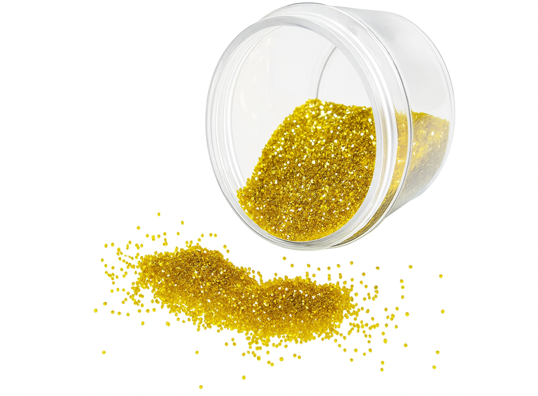
**Boron-doped diamond is a synthetic diamond material where boron atoms replace some carbon atoms. This process changes it from an electrical insulator into a conductor while keeping its physical strength. It comes in two main forms: powder and thin films.**

I consider boron-doped diamond to be one of the most cutting-edge products in the materials market today. It is not just a rock; it is a tool. When we talk about BDD, we are usually talking about two specific types. The first type is boron-doped powder. This looks like grey or black dust. The second type is boron-doped film. This is a coating that sits on top of another material.
I have noticed that widespread application is still in the exploration phase. There are two main reasons for this. First, the price is very high. It costs a lot to make a diamond that conducts electricity. Second, there are very few manufacturers who can actually make this product. It requires very specific technology.
Many universities and frontier research fields are currently studying it. I know of a university in China that has been researching this for a long time. They are looking at the conductivity of nano-grade and micron-grade diamonds. They want to see how well different sizes work. This research is vital because it helps us understand how to use the material better.
### Types of Boron-Doped Diamond
| Type | Description | Common Use |
| :— | :— | :— |
| **BDD Powder** | Loose particles, grey/black color. | Additive for resins, grinding wheels. |
| **BDD Film** | Solid layer grown on a substrate. | Electrodes, sensors, water treatment. |
The scarcity of producers means that if you can get your hands on high-quality BDD, you have a significant advantage. It is a specialized material for specialized problems.
## What is the structure of boron-doped diamond?
You cannot understand its power without looking inside the atomic makeup. Ignoring the atomic structure makes the material seem like magic. This leads to poor application choices and wasted resources.
**The structure consists of a standard diamond cubic lattice made of carbon atoms. However, boron atoms are substituted into specific spots within this grid. This substitution creates “holes” in the electron structure, which allows electrical current to move freely through the crystal.**

To understand the structure, you have to imagine a standard diamond first. In a normal diamond, every carbon atom holds hands with four other carbon atoms. They hold on very tight. This is what makes diamond so hard. It is also why electricity cannot get through. There is no room for electrons to move. The structure is locked down.
When we make boron-doped diamond, we force boron atoms into this group. Boron is slightly smaller than carbon. More importantly, it has one less electron than carbon. When a boron atom takes the place of a carbon atom, there is a missing electron. We call this missing spot a “hole.”
### The Role of the “Hole”
This “hole” is the secret. It acts like a positive charge. When you apply voltage, electrons from nearby atoms jump into the hole. This leaves a new hole behind them. As the electrons jump, current flows.
* **P-Type Semiconductor:** Because the current is carried by these positive holes, we call BDD a p-type semiconductor.
* **Doping Level:** The more boron you add, the more holes you create. If you add enough boron, the diamond acts almost like a metal wire.
I find this structure fascinating because we are hacking nature. We take the strongest structure known to man and modify it just enough to let power flow through it. It keeps the strength of the carbon bonds but gains the utility of the boron holes.
## What are the key properties of boron-doped diamond?
Engineers often choose materials that break easily or corrode in acid. This wastes money and time on constant repairs. You need something that survives harsh conditions while doing its job.
**BDD offers a unique combination of extreme hardness, high thermal conductivity, and chemical inertness. Crucially, it adds electrical conductivity and a wide electrochemical potential window. This means it can conduct electricity without reacting with the chemicals around it, even in strong acids.**
%[Properties chart of boron-doped diamond](https://placehold.co/600×400 “Key properties of BDD”)
The properties of BDD are what make it so expensive and so desirable. I want to break down the most critical features that I look for when testing this material.
### Electrical Conductivity
This is the main reason we buy it. The conductivity changes based on how much boron is inside. I have seen research from that Chinese university I mentioned earlier. They found that the conductivity varies greatly depending on the particle size and doping concentration. You can get BDD that is a semi-conductor, or you can get BDD that is highly conductive, almost like metal.
### Chemical Stability
This is my favorite property. You can put BDD in very strong acid, and it will not dissolve. Most metals would melt away. This makes BDD perfect for harsh environments. It has a “wide electrochemical potential window.” In simple terms, this means you can run a lot of voltage through it in water, and it will not break the water down into hydrogen and oxygen immediately. It waits until the voltage is very high. This allows it to destroy pollutants instead of just making bubbles.
### Physical Hardness
Even though we added boron, it is still a diamond. It is still harder than almost anything else. It resists scratching and wearing down.
| Property | Benefit |
| :— | :— |
| **Conductivity** | Allows electricity to flow for sensors and electrodes. |
| **Inertness** | Withstands acids and bases without corroding. |
| **Hardness** | Lasts a very long time without physical wear. |
| **Thermal** | Moves heat away quickly to prevent overheating. |
## What preparation methods are used for boron-doped diamond?
Making this material is not simple like baking a cake. If you use the wrong method, the quality fails instantly. This results in useless dust instead of high-tech material.
**The most common method is Chemical Vapor Deposition (CVD). In this process, gas mixtures containing carbon and boron are heated until they break down. The atoms then settle onto a surface, building the diamond layer by layer with the boron trapped inside.**

I mentioned earlier that there are few manufacturers. The reason is the difficulty of the preparation methods. You generally have two ways to do this, and both require expensive equipment.
### Chemical Vapor Deposition (CVD)
This is the most popular method for making films. Imagine a chamber filled with gas. Usually, we use methane for carbon and diborane for boron. We heat this gas up to extreme temperatures using microwaves or hot filaments. The gas breaks apart. The carbon and boron atoms rain down onto a substrate (like a silicon wafer). They land and form a diamond structure. Because the boron gas was mixed in, the boron atoms get trapped inside the crystal lattice. This grows the diamond layer by layer.
### High Pressure High Temperature (HPHT)
This method is more like how nature makes diamonds. We take graphite and a boron source. We put them in a massive press. We squeeze them with incredible pressure and heat them up. This crushes the carbon into diamond. This method is often used to make the powder form of BDD.
**Why is it so hard?**
You have to control the amount of boron perfectly. If you add too little, it does not conduct electricity. If you add too much, the crystal structure breaks, and it is no longer a diamond. It is a delicate balance. This complexity keeps the price high and limits the number of suppliers.
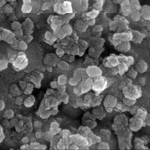
## What particle sizes are commonly available for boron-doped diamond?
One size does not fit all in industrial applications. Using the wrong particle size ruins the conductivity and the finish. This leads to project failure and wasted materials.
**BDD is available in a range of sizes from nanometers to microns. Nano-sized particles are used for fine coatings and precision electronics. Micron-sized particles are better for heavy-duty grinding tools that also need to dissipate static electricity.**
%[Comparison of nano and micro diamond particles](https://placehold.co/600×400 “Particle sizes of BDD”)
When I look at the market, I see a clear split in particle sizes. The size you choose depends entirely on what you want to do. The research from universities often focuses on how these sizes change performance.
### Nano-Scale Particles
These are tiny. You cannot see them with your eyes.
* **Size:** usually 10 to 100 nanometers.
* **Use:** These are great for mixing into inks or lubricants. Because they are so small, they have a massive surface area. This helps with chemical reactions. I have seen these used in medical sensors where space is very limited.
### Micro-Scale Particles
These are larger, like grains of sand or dust.
* **Size:** usually 1 to 100 microns.
* **Use:** These are used for rougher applications. If you are making a grinding wheel that needs to be conductive to prevent static shock, you use these. They are cheaper than the nano version usually.
### The Conductivity Difference
The Chinese university research I read highlighted an interesting point. The conductivity mechanisms work differently at these scales. In nano-diamonds, the electricity often jumps between the particles. In micro-diamonds, the electricity flows through the bulk of the crystal. This means you have to mix them differently to get the result you want.
| Size Category | Typical Range | Best Application |
| :— | :— | :— |
| **Nano** | < 100 nm | Biosensors, conductive inks, fine polishing. |
| **Micro** | > 1 um | Electrodes, grinding wheels, heat spreaders. |
## What are the application fields of boron-doped diamond?
Many industries are stuck using old, inefficient electrodes. These wear out fast and pollute the water they try to clean. You need a cleaner, longer-lasting solution.
**The primary applications are in wastewater treatment and electrochemical sensors. BDD electrodes break down organic pollutants in water efficiently. It is also used in biosensors to detect specific chemicals and in the disinfection industry because it generates powerful cleaning agents.**
%[Wastewater treatment using BDD electrodes](https://placehold.co/600×400 “Applications of BDD”)
Because BDD is a “frontier product,” we are still finding new ways to use it. However, there are three fields where it is already making a huge impact.
### Wastewater Treatment
This is the biggest application I see right now. factories produce water full of toxic organic dyes and chemicals. Traditional filters cannot catch everything. BDD electrodes are amazing here. When you put them in water and turn on the power, they create “hydroxyl radicals.” These are very aggressive molecules. They attack the pollutants and turn them into harmless carbon dioxide and water. It is a clean way to clean.
### Disinfection
This is related to the insight I shared. BDD films are used in disinfection. Because they can generate ozone and other sanitizing agents directly from the water, you do not need to buy bleach. You just need a BDD device and electricity. I have seen small home devices that use this to clean vegetables.
### Sensors
Because BDD does not react with chemicals, it creates a very “quiet” background for electrical signals. This makes it sensitive. It can detect tiny amounts of DNA or drugs in a blood sample. It is much better than carbon or gold electrodes for this.
* **High-End Manufacturing:** It is also used in Electrical Discharge Machining (EDM) as a wear-resistant electrode.
## How to select the appropriate boron-doped diamond?
Buying the wrong type of diamond is an expensive mistake. You might pay for features you do not need or get a product that fails. This hurts your budget significantly.
**To select the right BDD, you must look at the doping concentration and particle size. Higher boron content means better conductivity but slightly lower hardness. You must also decide between powder for additives or solid film for electrodes based on your specific device.**
%[Checklist for selecting boron-doped diamond](https://placehold.co/600×400 “Selecting the right BDD”)
Selecting the right material is difficult because there are few standards. Here is how I approach the problem when I need to choose a supplier or a grade.
### 1. Define Your Form
Do you need a powder or a solid piece?
* If you are making a **coating or ink**, you need **powder**.
* If you are building a **reactor or sensor**, you need **film** (CVD).
### 2. Check the Boron Concentration
This is usually measured in parts per million (ppm).
* **Low Doping:** Acts like a semiconductor. Good for transistors.
* **High Doping:** Acts like a metal. Good for electrodes and wastewater treatment.
* *Warning:* As you add more boron, the crystal gets more “defects.” It might become slightly more brittle. You have to balance conductivity with strength.
### 3. Consider the Price and Supplier
Since there are few manufacturers, prices vary wildy. You should ask for samples first. Test the conductivity yourself. I always advise checking if the supplier creates the material themselves or just resells it. Direct manufacturers usually offer better technical support.
### Selection Matrix
| Need | Recommended Choice |
| :— | :— |
| **Water Treatment** | High-doped CVD Film (Solid Plate) |
| **Conductive Glue** | Nano-sized BDD Powder |
| **Grinding Tool** | Micro-sized BDD Powder |
| **Bio-Sensor** | High-quality, smooth CVD Film |
## Conclusion
Boron-doped diamond is a powerful tool that turns standard diamond into an electrical conductor. Whether for cleaning water or advanced sensors, its unique structure solves problems other materials cannot.